|
|
|
|
|
|
|
|
|
|
|
|
|
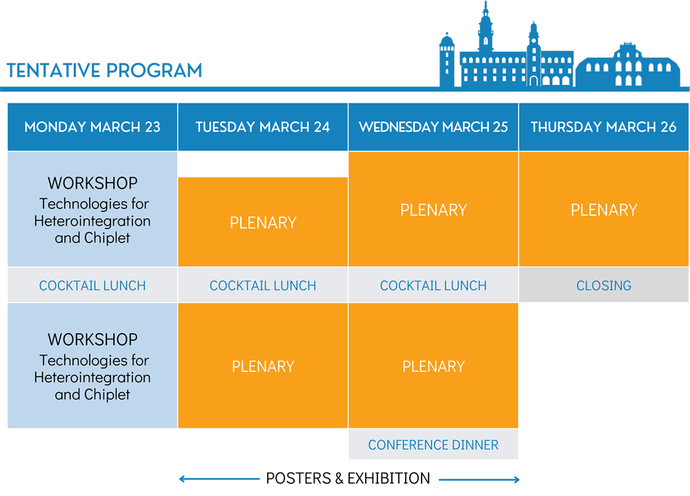
Tue 24 |
|
Wed 25 |
|
Thu 26 |
|
|
|
|
|
|
|
|
|
|
|
|
|
|
|
|
|
|
|
|
|
|
|
|
|
|
|
Workshop “Technologies for heterointegration and chiplets” |
|
|
|
|
|
|
|
|
|
|
|
|
|
|
|
|
|
|
|
|
|
|
|
|
|
|
|
|
|
10:30-10:45 |
|
Welcome and Opening |
|
|
|
|
|
|
|
|
|
|
|
|
|
|
|
|
Chairperson: To be defined |
|
|
|
|
|
|
|
|
|
|
|
|
|
|
|
10:45-11:30 |
|
INVITED |
|
Challenges and opportunities of 3D system integration |
|
Gerald Beyer,
imec, Belgium |
|
|
|
|
|
|
|
|
|
|
|
|
|
|
|
|
|
|
11:30-12:15 |
|
INVITED |
|
How wafer direct bonding mechanism enables die-to-wafer technology |
|
Frank Fournel,
CEA-LETI, France |
|
 |
|
|
|
|
|
|
|
|
|
|
|
|
|
|
|
|
|
|
|
|
|
|
|
|
|
|
|
|
|
|
Chairperson: To be defined |
|
|
|
|
|
|
|
|
|
|
|
|
|
|
|
13:15-14:00 |
|
INVITED |
|
Low temperature metallic wafer level bonding with selective heat input |
|
Klaus Vogel,
Fraunhofer ENAS, Germany |
|
|
|
|
|
|
|
|
|
|
|
|
|
|
|
|
|
|
14:00-14:45 |
|
INVITED |
|
Wafer level technologies for Heterointegration of Photonics Modules |
|
Stéphane Bernabé,
CEA-LETI, France |
|
|
|
|
|
|
|
|
|
|
|
|
|
|
|
|
|
|
|
|
|
|
|
|
|
|
|
|
|
|
|
|
Chairperson: To be defined |
|
|
|
|
|
|
|
|
|
|
|
|
|
|
|
15:15-16:00 |
|
INVITED |
|
Interconnects for Heterointegration schemes on Wafer and Panel level |
|
Jens Stolze,
Applied Materials Europe, Germany |
|
|
|
|
|
|
|
|
|
|
|
|
|
|
|
|
|
|
16:00-16:45 |
|
INVITED |
|
Multi-scale thermo-mechanics for electronics packaging |
|
Nathanael Joehrmann,
TU Chemnitz, Germany |
|
|
|
|
|
|
|
|
|
|
|
|
|
|
|
|
|
|
16:45-16:55 |
|
Closing Remarks |
|
|
|
|
|
|
|
|
|
|
|
|
|
|
|
. |
|
|
|
|
|
|
|
|
|
|
|
|